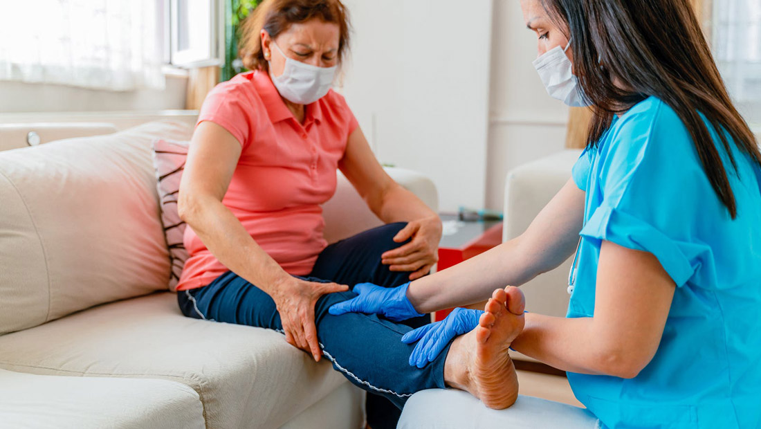
Observation of bulk-edge correspondence in topological pumping based on a tunable electric circuit
Electric LC resonators to emulate the Harper-Hofstadter-Hatsugai model
The features of two-dimensional electrons on a square lattice in a magnetic field with NN (ta and tb in x– and y-directions, respectively) and NNN (tc’) hoppings, called the Harper-Hofstadter-Hatsugai (HHH) model25,34, can be implemented as a one-dimensional system through the dimensional reduction25,34, that is, one of the components of the two-dimensional momentum is replaced with cyclic time. We show that the classical analog of the HHH model can be synthesized in a tunable one-dimensional electric circuit by modulating capacitances or inductances appropriately.
Here, we consider a lossless electric circuit consisting of N nodes and the corresponding LC resonators, where neighboring LC resonators are coupled. According to Kirchhoff’s law, the current I and the voltage V satisfy23,35
$${{{{{\bf{I}}}}}}=\left(i\omega C+\frac{1}{i\omega }W\right){{{{{\bf{V}}}}}},$$
(1)
where C and W are the N × N matrices of capacitances and the inverse of inductances of the circuit, and I and V are the N-vectors. ω is the angular frequency of alternating current. The HHH model can be implemented in either of the two cases; the first case has a fixed inductance and various capacitances of the circuit, and the second case has a fixed capacitance and various inductances. Here, we select the first case for the use of the advantages of variable capacitors that have been widely used in electric circuits, as shown in Fig. 1a, i.e., the system of Fig. 1a consists of N nodes and the corresponding resonators with each resonator having a constant inductance L0 and a variable capacitance \({C}_{j}\left(1\le\, j\le N\right)\). The neighboring jth and \((j+1){{{{{\rm{th}}}}}}\) resonators are capacitively coupled by the capacitance \({C}_{j,j+1}\). C0,1 is the capacitance between node 1 and the ground through jumper 2. In the periodic boundary condition (PBC), jumper 1 has the short connection with jumpers 2 and 3 being opened. Likewise, in the open boundary condition (OBC), jumpers 2 and 3 have the short connections with jumper 1 being opened.
a Circuit diagram consisting of N = 89 LC resonators with neighboring resonators being coupled capacitively. N, L0, Cj, Cj, j+1, and In are the number of LC resonators, the inductance of the inductors, the capacitance of the jth LC resonator, the capacitance between the jth and the (j+1)th nodes, and the current flowing into node n from outside of the node, respectively. The periodic boundary condition (PBC) is imposed by having jumper 1 to be short connection with jumpers 2 and 3 being opened. Likewise, the open boundary condition (OBC) is imposed by having jumpers 2 and 3 be short connections with jumper 1 being opened. b Fabricated circuit. LC resonators are coupled in series, which is indicated by the dashed line. The capacitances of variable capacitors were controlled by DC bias voltages supplied from the multi-channel D/A boards. The circuit system is implemented on a 40 cm × 45 cm FR4 board. The top layer of the circuit board contains signal lines and circuit components. The bottom layer has the ground plane and bias voltage lines for the control of variable capacitors. The impedance probe is connected to a node by using a coaxial cable. c Unit cell of the circuit. Wire-wound inductors, ceramic capacitors, and variable capacitors are mounted. Each LC resonator has a node connector to measure the impedance between the corresponding node and the ground.
Under the constant inductance L0, Eq. (1) is then rewritten as
$${{{{{\bf{I}}}}}}=i\omega {C}_{0}\left[H-\frac{{\omega }_{0}^{2}}{{\omega }^{2}}E\right]{{{{{\bf{V}}}}}},$$
(2)
where
$$H=\frac{1}{{C}_{0}}\left[\begin{array}{cccccc}{C}_{1}+{C}_{0,1}+{C}_{1,2} & -{C}_{1,2} & 0 & \ldots & 0 & -{{DC}}_{N,N+1}\\ -{C}_{1,2} & {C}_{2}+{C}_{1,2}+{C}_{2,3} & -{C}_{2,3} & \cdots & \cdots & 0\\ 0 & -{C}_{2,3} & \ddots & \cdots & \cdots & \cdots \\ \vdots & 0 & \vdots & \ddots & \cdots & \cdots \\ 0 & \vdots & \vdots & \vdots & \ddots & {-C}_{N-1,N}\\ -D{C}_{N,N+1} & \vdots & \vdots & \vdots & -{C}_{N-1,N} & {C}_{N}+{C}_{N-1,N}+{C}_{N,N+1}\end{array}\right],$$
(3)
and \({\omega }_{0}=1/\sqrt{{L}_{0}{C}_{0}}\). (We have normalized the matrix H by the capacitance C0.) E is the identity matrix. The boundary condition is periodic (open) when \(D=1(D=0)\). Note that \({C}_{{{{{\mathrm{0,1}}}}}}+{C}_{N,N+1}\) holds when imposing the PBC. We set the capacitances in the diagonal and non-zero off-diagonal components so that they satisfy \(\big({C}_{j}+{C}_{j-1,j}+{C}_{j,j+1}\big)/{C}_{0}=-2{t}_{a}{\cos }\left(\frac{2{{{{{\rm{\pi }}}}}}}{T}\tau +2{{{{{\rm{\pi }}}}}}\phi j\right)+{const}.\) and \({C}_{j,j+1}/{C}_{0}=-{t}_{b}\left\{1-2{t}_{c}{\cos }\left(\frac{2{{{{{\rm{\pi }}}}}}}{T}\tau +2{{{{{\rm{\pi }}}}}}\phi j+{{{{{\rm{\pi }}}}}}\phi \right)\right\}\), respectively, to emulate the HHH model. Here, const. stands for an offset value for those capacitances to be positive. The parameters τ, T, ϕ, and tc are the adiabatic parameter (regarded as time variable10,14), the period of the adiabatic parameter, the magnetic flux, and the NNN hopping amplitude normalized by tb (tc = tc’/tb), respectively.
In an electric circuit, the local density of states in quantum systems is evaluated by measuring the real part of the impedance at node n with other nodes being opened. The real part of the impedance at n node Zn is expressed as21
$${{{{{\rm{Re}}}}}}\left[{Z}_{n}\left(\omega +i0\right)\right]=\frac{1}{2f{C}_{0}}{\sum }_{i}{\delta }\left({\lambda }_{i}^{H}-\frac{{\omega }_{0}^{2}}{{\omega }^{2}}\right){\left|{\psi }_{i,n}\right|}^{2},$$
(4)
where \({\lambda }_{i}^{H}\) and \({\psi }_{i,n}\) are the eigenvalue and the nth component of the ith eigenmode of H, respectively. f is the frequency \(\omega /2{{{{{\rm{\pi }}}}}}\). The detail of the derivation of Eq. (4) is described in Supplementary Note 4.
Figure 1b, c shows the top view and the unit cell of the fabricated circuit. Wire-wound inductors, ceramic capacitors, and variable capacitors are mounted on a FR4 board, and N = 89 LC resonators are coupled in series (represented by the red dashed line). The capacitances are tuned by DC bias voltages supplied from the multi-channel digital to analog (D/A) converter boards, so that the capacitances are distributed to emulate the HHH model.
Observation of edge states near the topological phase transition
We now turn to our experimental results. As shown above, the local density of states at node n is evaluated by measuring the impedance at the node. In order to observe spectra for the bulk and topological edge states, we select nodes 1, 44, 45, and 89 for measuring the impedances, where we assume that nodes 1 and 89 correspond to the left-edge and the right-edge, respectively, and the average of the impedances at nodes 44 and 45 correspond to the bulk. We vary τ from 0 to 1 with ϕ = 1/2 fixed in the OBC. First, we set the NNN hopping parameter as tc = 0.1. Figure 2a–c show the impedance maps of the bulk, the left-edge, and the right-edge, respectively. We observe the gap around 0.96(ω0/ω)2 in the bulk (white horizontal dashed line, Fig. 2a). On the other hand, there are states at τ = 0.75 for the left-edge (Fig. 2b) and at τ = 0.25 for the right-edge (Fig. 2c) at 0.96(ω0/ω)2 (white horizontal dashed line, Fig. 2b, c), respectively. Figure 2d shows the impedance spectra of the three cases at τ = 0.25. We clearly observe the strong peak in the impedance of the right-edge and small impedances of the left-edge and the bulk at 0.96(ω0/ω)2. Similarly, for τ = 0.75, there is the strong peak in the impedance of the left-edge and small impedances of the right-edge and the bulk at the same frequency (τ = 0.75 in Fig. 2a–c). Therefore, we conclude that the left- and right-edge states are observed at τ = 0.75 and τ = 0.25, respectively.
a–c Impedance maps in the τ-(ω0/ω)2 space for tc = 0.1, where τ, ω0, ω, and tc are the adiabatic parameter, the normalizing angular frequency, the angular frequency, and the next-nearest-neighbor hopping parameter, respectively. d Impedance spectra for tc = 0.1 and τ = 0.25. e–g Impedance maps for tc = −0.1. h Impedance spectra for tc = −0.1 and τ = 0.25. In a, e, the averages of nodes 44 and 45 (bulk, the color bars show \(2f{C}_{0}{{\mbox{Re}}}\left\{\left[{Z}_{44}\left(\omega \right)+{Z}_{45}\left(\omega \right)\right]/2\right\}\)) are shown, where f, C0 and Zn (ω) are the frequency, the normalizing capacitance and the impedance at ω on node n. b, f show impedance maps on node 1 (left-edge, the color bars show \(2f{C}_{0}{{\mbox{Re}}}\left[{Z}_{1}\left(\omega \right)\right]\)). c, g Show impedance maps on node 89 (right edge, the color bars show \(2f{C}_{0}{{\mbox{Re}}}\left[{Z}_{89}\left(\omega \right)\right]\)). The dashed lines in a–c and e–g are the pseudo-Fermi energy.
The topological phase transition implies the change of the behaviors of edge states. To see this, we invert the sign of tc as \(0.1\to -0.1\). The results are shown in Fig. 2e–g. As in the case of tc = 0.1, we observe the gap around 0.96(ω0/ω)2 in the bulk [white horizontal dashed line, (Fig. 2e). Contrary to the case of tc = 0.1, there are states at τ = 0.25 for the left-edge (Fig. 2f) and at τ = 0.75 for the right-edge (Fig. 2g) at 0.96(ω0/ω)2 (white horizontal dashed line, Fig. 2f, g), respectively. Figure 2h shows the impedance spectra of the three cases at τ = 0.25. We clearly observe the strong peak in the impedance of the left-edge state and small impedances of the right-edge state and the bulk state. Thus, the left- and right- edge states are observed at τ = 0.25 and τ = 0.75, respectively. This means that the locations of edge states have flipped by the topological transition from tc = 0.1 to −0.1.
Here, we deduce the topological numbers of the edge states Iedge. We assume the “virtual Fermi energy” in the gap of 0.96(ω0/ω)2 (white horizontal dashed line, Fig. 2a–c, e–g). In the case of tc = 0.1, as τ increases, eigenvalues of the right-edge state decrease across the virtual Fermi energy at τ = 0.25, i.e., the right-edge state becomes occupied. Likewise, eigenvalues of the left-edge state increase across the virtual Fermi energy at τ = 0.75, i.e., the right-edge state becomes unoccupied. According to the theory of the topological pumping13, \({I}_{{{{{\rm{edge}}}}}}=1\) is determined from the edge state for the case of tc = 0.1. On the contrary, the left-edge state becomes occupied at τ = 0.25 and the right-edge state becomes unoccupied at τ = 0.75 when tc is inverted as \(0.1\to -0.1\). Thus, \({I}_{{{{{\rm{edge}}}}}}=-1\) is determined for the case tc = −0.1.
We note that our result is consistent with the behavior of the massive Dirac fermion36. Theoretically, the edge state has a linear dispersion in a bulk gap when the gap is opened, which is the feature of the massive Dirac fermion36,37,38. The similar feature is observed in our experiment. The edge states in our experiment have approximately linear dispersions crossing the virtual Fermi energy, and the sign of the derivative of the dispersions on τ at the same node is inverted in the topological transition.
Observation of bulk Chern numbers in the topological phase transition
In the previous section, we observed the topological phase transition by the edge states under the OBC. Here we extract the bulk Chern numbers from experimental impedance spectra of the Hofstadter butterfly under the PBC by employing Středa’s formula. We will show that the bulk Chern numbers are consistent with topological numbers obtained from the edge states.
We vary the flux parameter ϕ = p/q, where the integer p is varied from 1 to 88 with q = 89 fixed. For each p, impedance spectra for all N = 89 nodes are measured. The details of the measurements are presented in Methods. We have experimentally measured the impedance spectra \(2f{C}_{0}\mathop{\sum }\nolimits_{n=1}^{89}{{{{\rm{Re}}}}}\left[{Z}_{n}\left(\omega \right)\right]\). The impedance spectra for all p values are mapped in Fig. 3a, c, e for tc = 0, 0.1, and −0.1, respectively. Clear contrast of high impedance (bright color) to low impedance (dark color) is observed even in regions of higher-order gaps of the Hofstadter butterfly spectra. In the case of tc = 0, the Hofstadter butterfly map is symmetric with respect to \(\phi {{{{\rm{=}}}}}1{{{{\rm{/}}}}}2\). In the case of tc = 0.1, the center gap opens at ϕ = 1/2 and the large gap runs from the left to the right upwards (Fig. 3c). When the sign of the tc is inverted, the connection of the center gap of the Hofstadter butterfly switches and the large gap runs from the left to the right downwards (Fig. 3e). The butterfly spectra are well reproduced by numerical calculations and the circuit simulations (see Supplementary Note 2).
a Impedance maps as functions of (ω0/ω)2 and ϕ for tc = 0, where ω0, ω, ϕ, and tc are the normalizing angular frequency, the angular frequency, the flux parameter, and the next-nearest-neighbor hopping parameter, respectively. b \({\sum }_{i}^{{{\prime} }}{A}_{i}/\mathop{\sum}\nolimits_{i}{A}_{i}\) as a function of ϕ for tc = 0, where Σ’i and Ai are the summation below the gap we consider and the area of the ith Lorentzian, respectively. c Impedance map for tc = −0.1. d \({\sum }_{i}^{{{\prime} }}{A}_{i}/\mathop{\sum}\nolimits_{i}{A}_{i}\) as a function of ϕ for tc = 0.1. e Impedance map for tc = −0.1. f \({\sum }_{i}^{{{\prime} }}{A}_{i}/\mathop{\sum}\nolimits_{i}{A}_{i}\) as a function of ϕ for tc = −0.1. In a, c, e, the color bars show \(2f{C}_{0}{\sum }_{n=1}^{89}{{\mbox{Re}}}\left[{Z}_{n}\left(\omega \right)\right]\), where f, C0 and Zn (ω) are the frequency, the normalizing capacitance, and the impedance at ω on node n. The label in each of the maps in c, e represents the Chern number of the gap determined from d, f. Each value of \({\sum }_{i}^{{{\prime} }}{A}_{i}/\mathop{\sum}\nolimits_{i}{A}_{i}\) in d and f is obtained by the linear approximation from the corresponding hatched range of ϕ.
To extract the bulk Chen number \({C}_{{{{{\rm{bulk}}}}}}\), we employ the Středa’s formula39, ΔIDS/Δϕ = Cbulk, where IDS represents the integrated density of states which is the number of eigenvalues below the target gap divided by the total number of eigenvalues. For the lossless case, each eigenstate, in principle, appears as a peak in the impedance spectrum. However, in the presence of resistive loss, some of the eigenstates having a finite bandwidth are overlapped in a peak of the impedance. In order to count the number of eigenstates, we fit the spectra of \(2f{C}_{0}\mathop{\sum }\nolimits_{n=1}^{89}{{{{\rm{Re}}}}}\left[{Z}_{n}\left(\omega \right)\right]\) by using the Lorentzian function of \({\sum }_{{{{{{\rm{i}}}}}}}{A}_{{{{{{\rm{i}}}}}}}\frac{{a}_{i}}{{\pi }^{2}{\left[{\left({\omega }_{0}/\omega \right)}^{2}-{\left({\omega }_{0}/{\omega }_{{{{{{\rm{i}}}}}}}\right)}^{2}\right]}^{2}+{a}_{i}^{2}}\) where Ai, ai, and ωi represent the area of the Lorentzian, the half width at half maximum, and the peak angular frequency ωi of the ith peak. Thus, the number of eigenstates in a peak is counted by Ai even when some of those eigenstates are overlapped or degenerated. Therefore, \({\sum }_{i}^{{\prime} }{A}_{i}/\mathop{\sum}\nolimits_{i}{A}_{i}\) equivalently corresponds to the IDS, where Σ’ indicates the summation below the gap we consider. Examples of the approximated spectra are shown in the Supplementary Note 3. The least square method was used for the approximation of the Lorentzian curves, where the number and positions of spectral peaks are determined by the function findpeaks of MATLAB40 with Ai and ai being fitting parameters. First, we verify the derivation of bulk Chern numbers in the specific gaps of the butterfly using tc = 0, which are indicated by labels in Fig. 3a. The ϕ dependence of \({\sum }_{i}^{{\prime} }{A}_{i}/\mathop{\sum}\nolimits_{i}{A}_{i}\) below the target gaps is shown in the top panel of Fig. 3b. The bottom panel of Fig. 3b shows the residual of the approximation mentioned above, where the residual is calculated by integrating the deviation of the fitting curve from the experimental curve along (ω0/ω)2 with respect to the corresponding experimental area for each ϕ. In Fig. 3b, we observe that \({\sum }_{i}^{{\prime} }{A}_{i}/\mathop{\sum}\nolimits_{i}{A}_{i}\) exhibits a symmetric set of linear lines over the range of ϕ. This is the Wannier diagram41 and its global features are reproduced experimentally. Table 1 shows the summary of measured \(\frac{\Delta }{\Delta \phi }\left({\Sigma }^{{\prime} }{A}_{i}/\Sigma {A}_{i}\right)\) for each gap, where \(\Delta \phi =1/89\). We have retrieved the experimental values using linear functions from the hatched range of ϕ (\(5/89\le \phi \le 16/89,73/89\le \phi \le 85/89\)), where the residual of the spectra approximation is less than 0.05 (bottom panel of Fig. 2b). The experimental values (the 2nd row in Table 1) are almost integers for the gaps, which are consistent with the theoretical values25 (the 3rd row in Table 1). Therefore, deducing Chern numbers up to ±3 is confirmed. The deviation of the experimental values from the theoretical values may attribute to the accuracy of the accumulation \({\Sigma }^{{\prime} }{A}_{i}\) below the gap, i.e., high accuracy is obtained when the target gaps are located below 0.96 (ω0/ω)2 (the subscripts of labels are b and c) for Chern numbers of ±1, ±1, ±2, and ±3. We note that the residual is not small out of the hatched range of ϕ [bottom panel of Fig. 2b]. This can be related to the number of spectral peaks in the Lorentzian approximation. Namely, within the hatched region, e.g., at \(\phi =10/89\), the Lorentzian approximation has 9 peaks, and excellently agrees with the experimental spectrum (See Supplementary Fig. 3a). On the other hand, at \(\phi =30/89\), which is out of the hatched region, the Lorentzian approximation has only 3 peaks, and the discrepancy of the approximation curve from the experimental curve in the spectrum is pronounced (See Supplementary Fig. 3c).
Next, we deduced the bulk Chern number of the center gap across ϕ = 1/2 for the cases of tc = ±0.1. Figure 3d, f shows the corresponding \(\frac{\Delta }{\Delta \phi }\left({\Sigma }^{{\prime} }{A}_{i}/\Sigma {A}_{i}\right)\) as a function of ϕ below the center gap. The slops of the linearly approximated line in the hatched ranges are deduced to be 1.02 \(\left(6/89\le \phi \le 12/89\right)\) and 1.21 \(\left(76/89\le \phi \le 84/89\right)\) for tc = 0.1 (Fig. 3d), and −1.23 \(\left(4/89\le \phi \le 13/89\right)\) and −1.03 \(\left(74/89\le \phi \le 84/89\right)\) for tc = −0.1 (Fig. 3f), respectively, resulting in bulk Chern numbers of the center gap 1 and −1. The bulk Chern numbers are consistent with the topological numbers of the edge states, i.e., \({C}_{{{{{\rm{bulk}}}}}}={I}_{{{{{\rm{edge}}}}}}\). Therefore, we have experimentally confirmed the bulk-edge correspondence. In Ref. 25, bulk Chern numbers were theoretically obtained, and our results are consistent with the theoretical results.